Introduction
As the dimensions of processors continue to progressively diminish in pursuit of higher performance and greater integration, a concomitant increase in power density has been observed. This escalation in power density poses significant challenges in managing thermal dissipation and overall energy efficiency, thereby emphasizing the critical importance of effective power management strategies in modern electronic design. Consequently, reducing power consumption has emerged as a fundamental design parameter, particularly in the context of portable and mobile devices where constraints on size, weight, and battery life are paramount [1].
The importance of power efficiency is especially pronounced in mobile and handheld devices, including smartphones, tablets, and wearable technology, where the need for compact form factors and extended operational lifetime drives innovation in low-power circuit design. In such environments, the delicate balance between performance, size, and energy consumption necessitates the adoption of advanced techniques across multiple levels of system architecture. System designers have devised a multitude of strategies to mitigate dynamic power dissipation, encompassing innovations at the logic design level, architectural modifications, and enhancements in power management at the operating system layer [2].
This comprehensive review aims to elucidate the predominant techniques employed in the pursuit of power minimization. These methods include both classical and contemporary approaches, each with distinct advantages and limitations. Among the classical methods, the Voltage-Mode Bandgap Reference (VM-BGR) stands out as a widely utilized solution. The VM-BGR employs bipolar or CMOS transistors to generate a stable, temperature-independent reference voltage, which is crucial for ensuring consistent circuit operation across varying thermal conditions. However, the VM-BGR typically consumes more power relative to other techniques due to the biasing currents required for its operation.
In contrast, the Subthreshold Bandgap Reference represents an alternative approach that leverages transistors operating in the subthreshold region. This method significantly reduces power consumption, often reaching levels in the nanoampere range, making it particularly suitable for ultra-low-power applications. By operating in the subthreshold domain, the circuit exploits the exponential relationship between gate voltage and drain current, enabling the generation of stable reference voltages with minimal energy expenditure.
Overall, the ongoing advancements in power management techniques are vital for the development of energy-efficient electronic systems. These innovations not only extend battery life and improve thermal management but also contribute to the sustainability and reliability of modern electronic devices. As technology continues to evolve, the integration of these power reduction strategies will remain a central focus in the design of next-generation processors and systems [3].
Proposed algorithm:
It was decided to use the following scheme:
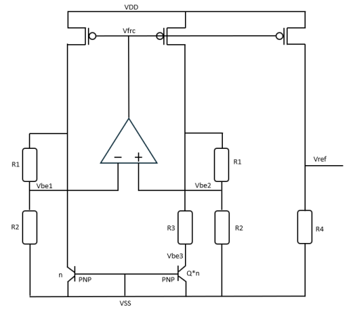
Fig. 1. Scheme of Low-Power Bandgap Reference
In subthreshold operation, Metal-Oxide-Semiconductor Field-Effect Transistors (MOSFETs) are biased at a gate-to-source voltage that is below the threshold voltage, enabling them to function in a region characterized by exponential current-voltage relationships. Although this mode has limitations in terms of speed and accuracy, it is very useful for ultra-low-power applications. Resistors R1 and R2, which act as a voltage divider, allow you to control the input voltage of the operational amplifier. Thus, by obtaining a constant current, the output voltage through the 2nd cascade can be determined using Ohm's law.
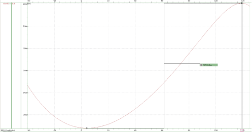
Fig. 2. The results obtained from the constant voltage source
This plot shows the output voltage of a designed constant-voltage source that has a very small voltage swing. Given the low supply voltage and the transistors going out of saturation, this approach made it possible to obtain CTAT and PTAT curves in the first cascade, while when using a high supply voltage this was done with the help of 2 cascades.
Results
Analytical results shown in table.
|
Power(μW) |
Area(μm²) | |
|
Reference circuit |
330 |
2000 |
|
Proposed circuit |
280 |
2400 |
Conclusion
Low-power bandgap references are essential components in energy-efficient integrated circuit design, especially in applications such as, mobile devices, sensor networks, implantable medical electronics. These circuits provide a temperature-independent stable reference voltage while consuming minimal power. In comparison with reference design power consumption decreased by 15 %, but area increased by 20 %.
References
- Behzad Razavi «Design of Analog CMOS Integrated Circuits» 2000
- R. Jacob Baker «CMOS Circuit Design, Layout and Simulation», Third Edition, 2010
- Chi-Wah Kok and Wing-Shan Tam «CMOS voltage references an analytic and practical perspective»